Lab 5A: Latches, Flip-flops, and Registers (Week 8)
Overview
This lab introduces sequential logic building blocks - circuits that have memory and can store state. You will learn the fundamental differences between latches and flip-flops, and how these building blocks are used to create registers.
Learning Objectives
After completing this lab, you will be able to:
- Understand the difference between combinational and sequential logic
- Learn the operation of SR latches and D latches
- Understand edge-triggered D flip-flops and their timing requirements
- Implement registers using flip-flops
- Understand synchronous vs asynchronous resets
Background: Sequential Logic Fundamentals
Combinational vs Sequential Logic
| Combinational Logic | Sequential Logic |
|---|---|
| Output depends ONLY on current inputs | Output depends on current inputs AND past history |
| No memory | Has memory (state) |
| No clock required | Usually requires clock |
| Examples: gates, MUX, decoder | Examples: latches, flip-flops, counters |
Why Sequential Logic?
Sequential circuits can:
- Store data (memory, registers)
- Count events (counters)
- Generate patterns (state machines)
- Synchronize operations (pipelining)
SR Latch
The Set-Reset (SR) Latch is the simplest memory element:
      ┌─────┐
  S ──┤ NOR ├──┬── Q
      └──┬──┘  │
         │     │
         └──┐  │
            │  │
      ┌──┬──┘  │
      │  │     │
  R ──┤ NOR ├──┴── Q̄
      └─────┘
SR Latch Truth Table
| S | R | Q (next) | Operation |
|---|---|---|---|
| 0 | 0 | Q | Hold (no change) |
| 0 | 1 | 0 | Reset |
| 1 | 0 | 1 | Set |
| 1 | 1 | X | Invalid (race condition) |
D Latch (Transparent Latch)
The D Latch eliminates the invalid state by using a single data input:
module d_latch (
    input  logic d,       // Data input
    input  logic enable,  // Enable (gate) signal
    output logic q        // Output
);

    always_latch begin
        if (enable)
            q = d;        // Transparent when enabled
        // When disabled, q retains its value
    end

endmodule
D Latch Behavior
- When
enable = 1: Q follows D (transparent) - When
enable = 0: Q holds previous value (latched)
⚠️ Problem: D latch is level-sensitive. Changes to D pass through as long as enable is high, making timing control difficult.
D Flip-Flop (Edge-Triggered)
The D Flip-Flop samples input only at the clock edge, providing precise timing control:
module d_ff (
    input  logic clk,     // Clock
    input  logic d,       // Data input
    output logic q        // Output
);

    always_ff @(posedge clk) begin
        q <= d;           // Sample D at rising edge only
    end

endmodule
Flip-Flop Timing Specifications
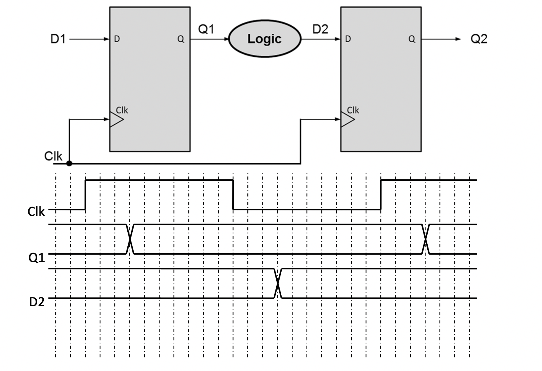
Figure 1: D Flip-Flop Timing Specifications
| Parameter | Symbol | Description |
|---|---|---|
| Setup Time | t_su | Time D must be stable BEFORE clock edge |
| Hold Time | t_hold | Time D must be stable AFTER clock edge |
| Clock-to-Q | t_cq | Delay from clock edge to Q change |
Timing Violation
If setup or hold time is violated, the flip-flop may enter a metastable state - an undefined state between 0 and 1 that can persist for an unpredictable time.
D Flip-Flop with Reset
Asynchronous Reset (Resets immediately)
module d_ff_async_rst (
    input  logic clk,
    input  logic rst_n,   // Active-low reset
    input  logic d,
    output logic q
);

    always_ff @(posedge clk or negedge rst_n) begin
        if (!rst_n)
            q <= 1'b0;    // Reset immediately
        else
            q <= d;
    end

endmodule
Synchronous Reset (Resets at clock edge)
module d_ff_sync_rst (
    input  logic clk,
    input  logic rst_n,   // Active-low reset
    input  logic d,
    output logic q
);

    always_ff @(posedge clk) begin
        if (!rst_n)
            q <= 1'b0;    // Reset at clock edge
        else
            q <= d;
    end

endmodule
When to Use Which Reset?
| Asynchronous Reset | Synchronous Reset |
|---|---|
| Works without clock | Requires clock to be running |
| Immediate response | Delayed by one clock |
| May cause glitches | Cleaner, glitch-free |
| Used for power-on reset | Used for functional reset |
Multi-bit Register
A register is simply multiple flip-flops sharing the same clock:
module register #(
    parameter WIDTH = 8
)(
    input  logic             clk,
    input  logic             rst_n,
    input  logic             en,       // Enable signal
    input  logic [WIDTH-1:0] d,
    output logic [WIDTH-1:0] q
);

    always_ff @(posedge clk or negedge rst_n) begin
        if (!rst_n)
            q <= '0;
        else if (en)
            q <= d;
        // else: hold value
    end

endmodule
Hardware Implementation
Top-Level Wrapper
module lab5a_top (
    input  logic       MAX10_CLK1_50,   // 50 MHz clock
    input  logic [9:0] SW,              // Switches
    input  logic [1:0] KEY,             // Push buttons (active low)
    output logic [9:0] LEDR             // LEDs
);

    logic clk, rst_n;

    assign clk   = MAX10_CLK1_50;
    assign rst_n = KEY[0];              // Reset button

    // 8-bit register demonstration
    register #(.WIDTH(8)) u_reg (
        .clk   (clk),
        .rst_n (rst_n),
        .en    (~KEY[1]),               // Load when KEY[1] pressed
        .d     (SW[7:0]),
        .q     (LEDR[7:0])
    );

    assign LEDR[9:8] = 2'b0;

endmodule
Verification
Simulation Testbench
module d_ff_tb;
    logic clk, rst_n, d, q;

    d_ff_async_rst uut (.*);

    // Clock generation: 10ns period
    initial clk = 0;
    always #5 clk = ~clk;

    initial begin
        // Initialize
        rst_n = 0; d = 0;
        #20;

        // Release reset
        rst_n = 1;
        #10;

        // Test pattern
        d = 1; #10;
        $display("After d=1: q=%b", q);

        d = 0; #10;
        $display("After d=0: q=%b", q);

        // Test reset
        rst_n = 0; #5;
        $display("During reset: q=%b", q);

        $finish;
    end
endmodule
Lab Manual
📄 Download Lab 5A Manual (PDF)
Deliverables
- SystemVerilog Design:
d_ff.sv,register.sv,lab5a_top.sv - Testbench: Verify reset and data loading
- Timing Diagram: Draw Q response to clock and data changes
- Hardware Demo: Demonstrate register operation on DE10-Lite
- Individual Screenshot: Show simulation waveforms
- Submission: Upload
lab5a_top.svffile
Key Takeaways
- Latches are level-sensitive, flip-flops are edge-triggered
- Setup and hold times must be satisfied to avoid metastability
- Use always_ff for flip-flops, always_latch for latches
- Use non-blocking assignments (
<=) in sequential blocks - Asynchronous reset for power-on, synchronous reset for logic control