Lab 4 – Four-bit, Error Correction Code (ECC) using Hamming(7,4) Code Decoding
Introduction
In Lab 2 you designed a Hamming(7,4) encoder. In this lab you will be designing for the reverse operation, i.e., a decoder. The input to the decoder will be a 7-bit Hamming code. The output will be the original 4-bit code. You will also be able to insert a 1-bit error in the input Hamming code and see that it gives the correct original code.
This technique can be used when transmitting data through an environment where only single bit errors are expected per word of data.
Hardware Implementation
In the hardware implementation, you will be defining test Hamming codes in your design by the setting of seven of the switches. You will observe the decoded binary output on four of the LEDs. If the code has a one-bit error, you will observe the index of the error bit on the seven-segment display. Therefore, you will need to reuse the seven-segment display decoder you designed in Lab 3.
Hamming Code Space
While the input has 128 possible codes (2⁷), only 16 are the error-free codes as shown in the table below (basically the reverse of Lab 2). The full 128 possible input codes are provided to you in the testbench text file, tb_lab4_decoder.txt.
| h_code[7:1] | decode[4:1] |
|---|---|
| 7’b0000000 | 4’b0000 |
| 7’b0000111 | 4’b0001 |
| 7’b0011001 | 4’b0010 |
| 7’b0011110 | 4’b0011 |
| 7’b0101010 | 4’b0100 |
| 7’b0101101 | 4’b0101 |
| 7’b0110011 | 4’b0110 |
| 7’b0110100 | 4’b0111 |
| 7’b1001011 | 4’b1000 |
| 7’b1001100 | 4’b1001 |
| 7’b1010010 | 4’b1010 |
| 7’b1010101 | 4’b1011 |
| 7’b1100001 | 4’b1100 |
| 7’b1100110 | 4’b1101 |
| 7’b1111000 | 4’b1110 |
| 7’b1111111 | 4’b1111 |
Table 1: Hamming(7,4) decode data
Hamming Code Implementation Details
In order to do 1-bit error correction and determine the bit in error, let’s look at the implementation details of the Hamming(7,4) code. From Lab 2 you recall that the code was put together as:
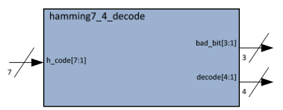
Figure: Hamming(7,4) code structure showing data and parity bit positions
e[7:1] = {d[4], d[3], d[2], p3, d[1], p2, p1}
It is pretty clear from this as to how to unwrap the data and parity bits. Since you used even parity to define p1, p2 & p3 in Lab 2, then the parity check (pc) operation (bits) should be:
pc1 = p1 xor d[1] xor d[2] xor d[4]
pc2 = p2 xor d[1] xor d[3] xor d[4]
pc3 = p3 xor d[2] xor d[3] xor d[4]
SystemVerilog Implementation
In SystemVerilog, we can implement the decoder using continuous assignments. First, extract the data and parity bits from the input:
module hamming7_4_decode(
    output logic [4:1] decode,
    output logic [3:1] bad_bit,
    input  logic [7:1] h_code
);

    // Extract data bits from h_code
    // h_code = {d[4], d[3], d[2], p3, d[1], p2, p1}
    logic [4:1] d;
    logic p1, p2, p3;

    assign d[4] = h_code[7];
    assign d[3] = h_code[6];
    assign d[2] = h_code[5];
    assign p3   = h_code[4];
    assign d[1] = h_code[3];
    assign p2   = h_code[2];
    assign p1   = h_code[1];

    // Parity check bits (bad_bit indicates error location)
    assign bad_bit[1] = p1 ^ d[1] ^ d[2] ^ d[4];
    assign bad_bit[2] = p2 ^ d[1] ^ d[3] ^ d[4];
    assign bad_bit[3] = p3 ^ d[2] ^ d[3] ^ d[4];

    // Output the decoded data
    assign decode = d;

endmodule
Key Point: The
^operator is the XOR operator in SystemVerilog.
Parity Check Matrix
Putting this information in a table form, where the highlighted bits are those used for the parity checking operation:
| Parity Check | e[7] (d[4]) | e[6] (d[3]) | e[5] (d[2]) | e[4] (p3) | e[3] (d[1]) | e[2] (p2) | e[1] (p1) |
|---|---|---|---|---|---|---|---|
| pc3 | d[4] | d[3] | d[2] | p3 | |||
| pc2 | d[4] | d[3] | d[1] | p2 | |||
| pc1 | d[4] | d[2] | d[1] | p1 |
Table 2: Parity Check matrix
Error Detection Logic
Here is the beauty of Dr. Hamming’s design. Observe the values of concatenated bits: {pc3,pc2,pc1}. If there are no bit errors in the input: h_code, the 3-bit parity check value is 3’b000. If the first bit (p1) is in error, the parity check value is 3’b001. If p2 is flipped, the check value is 3’b010. If d[1], 3’b011, and so on; thus, the 3-bit parity check code defines the binary index of the flipped bit.
Rather than use pc3, pc2 & pc1, we will combine/define these into a 3-bit signal: bad_bit[3:1] as illustrated in the table below. The input signal names in the table have also been converted to those used in this lab (h_code).
| Parity Check | h_code[7] | h_code[6] | h_code[5] | h_code[4] | h_code[3] | h_code[2] | h_code[1] |
|---|---|---|---|---|---|---|---|
| bad_bit[3] | h_code[7] | h_code[6] | h_code[5] | h_code[4] | |||
| bad_bit[2] | h_code[7] | h_code[6] | h_code[3] | h_code[2] | |||
| bad_bit[1] | h_code[7] | h_code[5] | h_code[3] | h_code[1] |
Table 3: Parity check matrix translated to bad_bit signals
Note: Finally, it is also pretty obvious that if two bits are flipped, the index does not correctly point to either of the bits in error.
Detailed Specification
This design will have seven input switches (sw[6:0]) that will define the 7-bit Hamming code to test your decoder’s input. The output of the decoder will drive:
- 4 LEDs that represent the 4-bit binary output data
- Seven-segment display showing the 3-bit parity check code on digit 0
To drive this display you will need to use the seven-segment decoder module from your previous lab.
Hardware Behavior
When implemented in hardware, you should be able to set the 7 switches to any of the Hamming codes defined in Table 1 and see the corresponding binary output decoded on the LEDs. For any of these 16 non-error codes, the seven-segment display digit should be zero.
Then toggle one bit at a time on the selected code and note how the display digit changes from zero to the bit index that you are changing. Thus, it is easy to imagine how using this information you could correct the bit in error and display the correct code.
Design/Module Structure
In this design you will need to work with three separate modules:
1. hamming7_4_decode Module
The main module that contains the basic design. This module decodes the 7 input bits to 7 output bits, consisting of:
- 4 bits of decoded data (Table 1)
- 3 parity check bits that point to the bit in error (Table 3)
2. svn_seg_decoder Module
Your seven-segment decoder from Lab 3. The Lab 4 project file automatically links your seven-segment decoder design from Lab 3. It does not link the testbench, since this design has already been verified in Lab 3.
3. lab4_decoder Module
The decoder wrapper. It instantiates these two modules into a single module that is finally instantiated in the top level I/O wrapper. The lab4_decoder module has:
- 7 input switches
- 4 LED output signals
- 11 output signals for the seven-segment display (4 anodes, 7 cathodes)
Signal Connections
Inside this module, a few signals are hardwired – or set to fixed levels:
- The signal driving the display_on from the instantiating of the seven-segment decoder is set to logic one so that the display is always on
- The signals selecting the anodes (an) are set so that only one digit is displayed
Block Diagrams
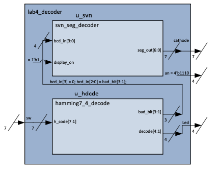
Figure: Lab 4 decoder block diagram showing module interconnections
Design Steps
-
Review Testbench File: The testbench file,
tb_hamming7_4_decode.txt, is provided to you based on the error-free truth table for the Hamming code as per Table 1, and expanded to include the error codes as well as the output bad_bit signals. Look over this text file, but do not change it. Note that because there are 7 input signals, there are 2⁷ = 128 possible combinations of this input pattern. -
Complete hamming7_4_decode Module: Complete the design for
hamming7_4_decodebased on this specification (equations above), including the bad_bit output signal. -
Complete lab4_decoder Module: Complete the design for
lab4_decoderthat instantiates this module and the seven-segment decoder into a single module and appropriately connects to the I/Os.
lab4_decoder Wrapper Template
module lab4_decoder(
    output logic [6:0] cathode,
    output logic [3:0] an,
    output logic [3:0] led,
    input  logic [6:0] sw
);

    // Internal signals
    logic [4:1] decode;
    logic [3:1] bad_bit;
    logic [3:0] bcd_in;
    logic [6:0] seg_out;

    // Instantiate Hamming decoder
    hamming7_4_decode u_hdcde (
        .decode(decode),
        .bad_bit(bad_bit),
        .h_code({sw[6:0]})  // Note: h_code is [7:1], sw is [6:0]
    );

    // Prepare BCD input for seven-segment decoder
    // Only display bad_bit value (0-7)
    assign bcd_in = {1'b0, bad_bit};

    // Instantiate seven-segment decoder
    svn_seg_decoder u_svn (
        .seg_out(seg_out),
        .bcd_in(bcd_in),
        .display_on(1'b1)   // Always on
    );

    // Output connections
    assign cathode = seg_out;
    assign an = 4'b1110;     // Only digit 0 is active (active-low)
    assign led = decode;     // Display decoded data on LEDs

endmodule
Important: Pay attention to the signal width mapping between
h_code[7:1]andsw[6:0]. You may need to adjust the connection accordingly.
Simulation/Verification
There are two testbench wrappers – one for each of the two above modules:
tb_hamming7_4_decode.svandtb_lab4_decoder.sv
Each of these has a text file (.txt) to provide the test vector data. Your seven-segment decoder was tested in Lab 3.
Simulation Commands
There are two simulation command files (right-click each of the *.m_sim files and Run) associated with the testbenches:
hamming7_4_decode.m_sim- to simulate and test the Hamming(7-4) decoder module alonelab4_decoder.m_sim- to simulate and test the integration of the decoder modules
Important: Remember to save a screen shot of each simulation log file for your reports. There will be two different simulation log files you will need.
Debugging
Use the .vcd waveform files to help debug your code if it doesn’t pass the simulations.
Synthesis and Hardware Testing
Generate Binary File
Generate a binary file as you did in past labs (right-click and Run on: lab4_top.qsf). When successful, you will generate the file: lab4_top.sof.
Hardware Testing
Copy it to your shared folder to load and run on your DE10-Lite board using the SVF Loader.
Test Procedure
- Insert some known error-free codes as defined in the truth table in the Introduction
- Observe the decoded 4-bit data on the LEDs
- Verify the seven-segment display shows “0” for error-free codes
- Switch some of the bits, one at a time and see how your display points to the bit (switch) in error
- Note that some of these will not be the data bits, but the check bits
Summary
| Component | Purpose |
|---|---|
hamming7_4_decode | Core decoder logic with error detection |
svn_seg_decoder | Seven-segment display driver (from Lab 3) |
lab4_decoder | Top-level wrapper integrating both modules |
| Testbenches | Verify decoder functionality and integration |
| Hardware | Switches for input, LEDs for output, seven-segment for error indication |
Deliverables
- Completed
hamming7_4_decode.svmodule - Completed
lab4_decoder.svwrapper module - Screenshot of
hamming7_4_decode.m_simsimulation results - Screenshot of
lab4_decoder.m_simsimulation results - Submission of
lab4_top.svffile - Hardware testing verification (error-free codes and single-bit error correction)