Lab 2: Encoder Design - Error Correction Code (Week 4)
Overview
In this lab, you will design a Hamming(7,4) encoder that takes 4 data bits and produces 7 output bits with error detection and correction capability. This is a fundamental concept in digital systems, memory design, and communications.
Learning Objectives
After completing this lab, you will be able to:
- Understand the concept of Error Correction Codes (ECC) and their importance
- Learn Hamming code encoding principles
- Implement a 4-bit to 7-bit encoder using XOR parity calculations
- Verify the encoder operation through simulation
Background: Hamming(7,4) Code
Why Error Correction?
Digital systems are susceptible to noise and interference that can cause bit errors. In critical applications (memory, storage, communication), we need mechanisms to detect and correct these errors.
Hamming Code Structure
The Hamming(7,4) code encodes 4 data bits (d3, d2, d1, d0) into 7 code bits by adding 3 parity bits (p2, p1, p0):
| Position | 7 | 6 | 5 | 4 | 3 | 2 | 1 |
|---|---|---|---|---|---|---|---|
| Bit | d3 | d2 | d1 | p2 | d0 | p1 | p0 |
Parity Bit Calculation
Each parity bit covers specific data bit positions:
p0 = d0 ⊕ d1 ⊕ d3    (covers positions 1, 3, 5, 7)
p1 = d0 ⊕ d2 ⊕ d3    (covers positions 2, 3, 6, 7)
p2 = d1 ⊕ d2 ⊕ d3    (covers positions 4, 5, 6, 7)
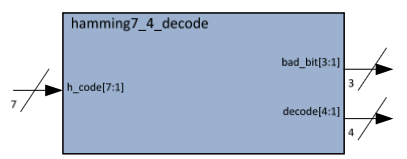
Figure 1: Hamming(7,4) Encoder Block Diagram
Design Specification
Block Diagram
            ┌───────────────────────────────────┐
    d[3:0]  │                                   │  code[6:0]
   ─────────┤       Hamming(7,4) Encoder        ├──────────
   (4 bits) │                                   │  (7 bits)
            └───────────────────────────────────┘
Module Interface
module hamming74_encoder (
    input  logic [3:0] data_in,     // 4 data bits: d3, d2, d1, d0
    output logic [6:0] code_out     // 7-bit Hamming code
);
Truth Table (Partial)
| d3 | d2 | d1 | d0 | p2 | p1 | p0 | code_out |
|---|---|---|---|---|---|---|---|
| 0 | 0 | 0 | 0 | 0 | 0 | 0 | 7’b0000000 |
| 0 | 0 | 0 | 1 | 0 | 1 | 1 | 7’b0000111 |
| 0 | 0 | 1 | 0 | 1 | 0 | 1 | 7’b0010101 |
| 0 | 1 | 0 | 0 | 1 | 1 | 0 | 7’b0101110 |
| 1 | 0 | 0 | 0 | 1 | 1 | 1 | 7’b1001111 |
| 1 | 1 | 1 | 1 | 1 | 1 | 1 | 7’b1111111 |
SystemVerilog Implementation
Template Code
module hamming74_encoder (
    input  logic [3:0] data_in,     // d3, d2, d1, d0
    output logic [6:0] code_out     // {d3, d2, d1, p2, d0, p1, p0}
);

    // Extract individual data bits for clarity
    logic d3, d2, d1, d0;
    logic p2, p1, p0;

    assign {d3, d2, d1, d0} = data_in;

    // Calculate parity bits using XOR
    assign p0 = d0 ^ d1 ^ d3;    // Parity for positions 1,3,5,7
    assign p1 = d0 ^ d2 ^ d3;    // Parity for positions 2,3,6,7
    assign p2 = d1 ^ d2 ^ d3;    // Parity for positions 4,5,6,7

    // Construct output: {d3, d2, d1, p2, d0, p1, p0}
    assign code_out = {d3, d2, d1, p2, d0, p1, p0};

endmodule
Alternative Using Continuous Assignment
module hamming74_encoder (
    input  logic [3:0] data_in,
    output logic [6:0] code_out
);

    assign code_out[0] = data_in[0] ^ data_in[1] ^ data_in[3]; // p0
    assign code_out[1] = data_in[0] ^ data_in[2] ^ data_in[3]; // p1
    assign code_out[2] = data_in[0];                           // d0
    assign code_out[3] = data_in[1] ^ data_in[2] ^ data_in[3]; // p2
    assign code_out[4] = data_in[1];                           // d1
    assign code_out[5] = data_in[2];                           // d2
    assign code_out[6] = data_in[3];                           // d3

endmodule
Hardware Implementation
Top-Level Wrapper
Your lab2_top.sv module should connect the encoder to the DE10-Lite switches and LEDs:
module lab2_top (
    input  logic [9:0] SW,      // Slide switches
    output logic [9:0] LEDR     // Red LEDs
);

    // Instantiate Hamming encoder
    // SW[3:0] → data input
    // LEDR[6:0] → encoded output

    hamming74_encoder u_encoder (
        .data_in  (SW[3:0]),
        .code_out (LEDR[6:0])
    );

    // Unused LEDs
    assign LEDR[9:7] = 3'b0;

endmodule
Pin Assignments
| Signal | FPGA Pin | Component |
|---|---|---|
| SW[0] | PIN_C10 | Switch 0 (d0) |
| SW[1] | PIN_C11 | Switch 1 (d1) |
| SW[2] | PIN_D12 | Switch 2 (d2) |
| SW[3] | PIN_C12 | Switch 3 (d3) |
| LEDR[0] | PIN_A8 | LED 0 (p0) |
| LEDR[1] | PIN_A9 | LED 1 (p1) |
| LEDR[2] | PIN_A10 | LED 2 (d0) |
| LEDR[3] | PIN_B10 | LED 3 (p2) |
| LEDR[4] | PIN_D13 | LED 4 (d1) |
| LEDR[5] | PIN_C13 | LED 5 (d2) |
| LEDR[6] | PIN_E14 | LED 6 (d3) |
Verification
Testing Procedure
- Set all switches OFF (0000) → LEDs should show 0000000
- Set SW[0] ON (0001) → LEDs should show 0000111
- Set SW[3] ON only (1000) → LEDs should show 1001111
- Try all 16 combinations and verify parity bits
Simulation Testbench
Create a testbench to verify all 16 input combinations:
module hamming74_encoder_tb;
    logic [3:0] data_in;
    logic [6:0] code_out;

    hamming74_encoder uut (.*);

    initial begin
        $display("Data In | Code Out | p2 p1 p0");
        $display("--------|----------|----------");

        for (int i = 0; i < 16; i++) begin
            data_in = i;
            #10;
            $display("  %b  |  %b  |  %b  %b  %b",
                     data_in, code_out,
                     code_out[3], code_out[1], code_out[0]);
        end

        $finish;
    end
endmodule
Lab Manual
Deliverables
- SystemVerilog Design:
hamming74_encoder.svandlab2_top.sv - Testbench:
hamming74_encoder_tb.sv - Simulation Waveform: Screenshot showing all 16 test cases
- Hardware Demo: Demonstrate encoder operation on DE10-Lite
- Individual Report: Include block diagram, code, and verification results
- Submission: Upload
lab2_top.svffile
Related Resources
- 📖 Wikipedia: Hamming(7,4) Code
- 📖 EDA Playground for Simulation
- ➡️ Lab 4: Hamming Decoder - The corresponding decoder design