Lab 1 – Introduction to Verilog HDL & the Lab Design Flow
Overview
In this lab, you will be introduced to the Verilog Hardware Description Language and the design flow we will be using in the labs throughout the course.
More specifically, the designs you produce and test will be written in SystemVerilog, a superset of Verilog that is both a Hardware Description Language (HDL) and Hardware Verification Language (HVL).
| File Type | Extension | Description |
|---|---|---|
| Verilog | .v | Traditional Verilog files |
| SystemVerilog | .sv | Enhanced Verilog with additional features |
All design files in this course will use the .sv extension. For our purposes, Verilog and SystemVerilog have essentially the same functionality, with SystemVerilog introducing the useful logic data type.
📖 Read more about Verilog vs SystemVerilog differences
Prerequisites (Lab 0)
Before starting this lab, ensure you have completed:
- AWS Cloud9 connection setup
- VS Code configured for remote access
- VirtualBox installed for hardware programming
- SSH keys generated and configured
All content for this lab is located in:
/home/<username>/ece2613/lab1
Note: Consult with a lab instructor if any prerequisites are incomplete.
DE10-Lite Hardware
The hardware you will be using is the DE10-Lite board, which contains an FPGA device manufactured by Intel (formerly Altera).
You have been supplied with:
- DE10-Lite FPGA board
- USB cable for programming
📄 Read more about DE10-Lite hardware (intel_altera_v1.pdf)
Basic Design Flow
The design flow for labs in this course consists of the following steps:
┌─────────────────────────────────────────────────────────────┐
│  1. Design Entry                                            │
│     Enter your design using SystemVerilog on AWS Cloud9     │
├─────────────────────────────────────────────────────────────┤
│  2. Simulation                                              │
│     Simulate and verify design is functionally correct      │
├─────────────────────────────────────────────────────────────┤
│  3. Synthesis                                               │
│     Create binary file (*.sof) for FPGA hardware            │
├─────────────────────────────────────────────────────────────┤
│  4. Download                                                │
│     Transfer binary file to local machine                   │
├─────────────────────────────────────────────────────────────┤
│  5. Hardware Test                                           │
│     Load binary into DE10-Lite and verify operation         │
└─────────────────────────────────────────────────────────────┘
The Design
For this lab, you need to design four different gates by instantiating the appropriate primitives.
Gate Types
You will implement the following gates:
- AND
- OR
- XOR
- NAND
Block Diagram
         ┌─────────┐
   a0 ───┤         │
         │  AND    ├─── f0
   b0 ───┤  (u1)   │
         └─────────┘

         ┌─────────┐
   a1 ───┤         │
         │  OR     ├─── f1
   b1 ───┤  (u2)   │
         └─────────┘

         ┌─────────┐
   a2 ───┤         │
         │  XOR    ├─── f2
   b2 ───┤  (u3)   │
         └─────────┘

         ┌─────────┐
   a3 ───┤         │
         │  NAND   ├─── f3
   b3 ───┤  (u4)   │
         └─────────┘
The inputs will be connected to switches and outputs to LEDs.
Truth Table
Complete the truth table for the gates in this design:
| a | b | AND (f0) | OR (f1) | XOR (f2) | NAND (f3) |
|---|---|---|---|---|---|
| 0 | 0 | 0 | 0 | 0 | 1 |
| 0 | 1 | 0 | 1 | 1 | 1 |
| 1 | 0 | 0 | 1 | 1 | 1 |
| 1 | 1 | 1 | 1 | 0 | 0 |
Design Entry
Step 1: Open the Project
- Open VS Code and connect to the AWS server
- Navigate to the
lab1folder - Open
gates.sv- this contains a skeleton of your design module
Step 2: Implement the Gates
Within gates.sv, instantiate each of the four primitive gates. You can use either method:
Method 1: Gate Primitives (Instantiation)
and u1 (f0, a0, b0);
or  u2 (f1, a1, b1);
xor u3 (f2, a2, b2);
nand u4 (f3, a3, b3);
Method 2: Continuous Assignment
assign f0 = a0 & b0;   // AND
assign f1 = a1 | b1;   // OR
assign f2 = a2 ^ b2;   // XOR
assign f3 = ~(a3 & b3); // NAND
📖 Examples of gate primitives 📖 Examples of gate operators
Step 3: Save Your Work
Save frequently using Ctrl+S!
Simulation
Simulation checks your design’s syntax and verifies it matches your specifications (the truth table above).
Self-Checking Testbench
A self-checking testbench is provided: tb_gates.sv
This testbench:
- Reads test vectors from
tb_gates.txt - Applies inputs to your design every 20 nsec
- Compares outputs to expected values
- Reports any mismatches
Running the Simulation
- Find the file
gates.m_simin your environment - Right-click on it and select Run
- Observe the terminal at the bottom of VS Code
- Check the log file:
tb_gates.log
Expected Result
You are looking for this message:
Simulation complete – no mismatches!!!
Important: Take a screenshot of this window for your lab report.
Fixing Errors
If you have mismatches, the testbench will display:
- Input values
- Expected outputs
- Your design outputs
Use this information to find and fix your design errors.
⚠️ You must correct all mismatches before continuing to hardware implementation!
Synthesis
Synthesis creates a binary file that can be loaded into your DE10-Lite board.
Step 1: Run Synthesis
- Find the file
lab1_top.qsfin your directory - Right-click on it and select Run
- Wait for the tool to optimize and map your design
Step 2: Locate the Output File
When synthesis completes without errors:
- Navigate to the
output_filesdirectory (refresh if needed) - Find the file:
lab1_top.svf
Note: The
.svf(Serial Vector Format) file is used for programming via the web loader.
Step 3: Download the File
- Right-click on
lab1_top.svf - Select Download
- The file will be saved to your local Downloads folder
Hardware Testing
Step 1: Connect the DE10-Lite Board
- Connect the DE10-Lite board to your PC via USB cable
- Ensure the board powers on (you should see LEDs light up)
Step 2: Open the SVF Loader
- Open your web browser (Chrome recommended)
- Navigate to: https://temple.short.gy/svfloader
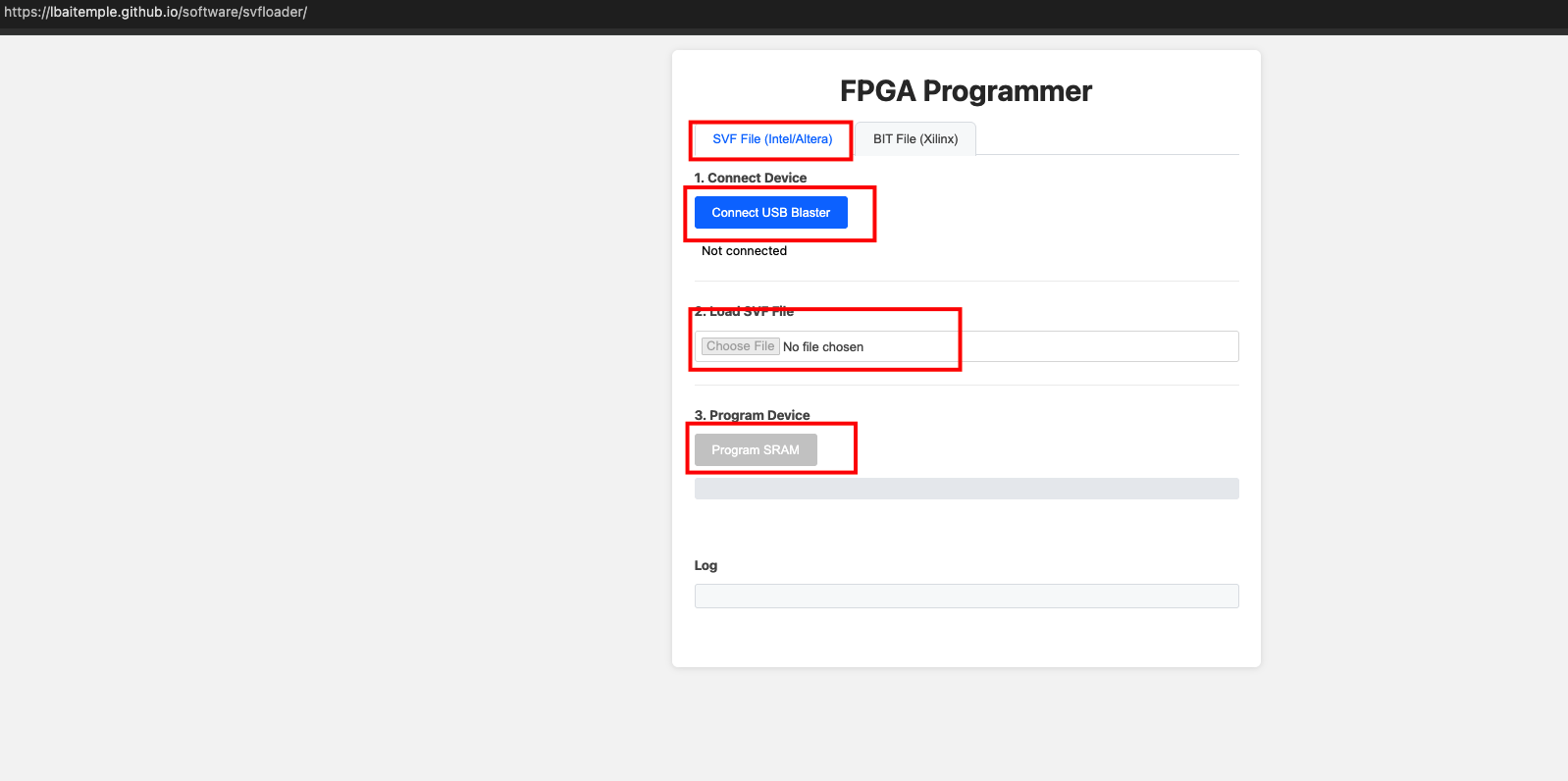
Figure: FPGA Programming Interface for DE10-Lite
Step 3: Load the Design
- Click the Choose File or Browse button on the webpage
- Select your
lab1_top.svffile from your Downloads folder - Click Upload or Program to load the design into the DE10-Lite
Note: The web-based SVF loader communicates directly with your DE10-Lite board through WebUSB. You may need to grant browser permissions to access the USB device.
Step 4: Verify Your Design
Test your design by:
- Toggling the switches (inputs)
- Observing the LEDs (outputs)
- Comparing behavior to your truth table
Questions to consider:
- Does the behavior match your expectations?
- Does it meet the design specifications?
Shutting Down
When finished:
- Close all open tabs in VS Code
- Close VS Code (disconnects from AWS server)
- Disconnect the DE10-Lite board from USB
Troubleshooting
| Issue | Solution |
|---|---|
| Design won’t load | Check USB connection in VirtualBox: Devices → USB → Ensure “Altera USB-Blaster [0400]” is checked |
| USB not recognized | Use USB 3.0 port (check in Device Manager → Universal Serial Bus controllers) |
| VirtualBox issues | Restart VirtualBox; connect DE10-Lite before starting VirtualBox |
| Driver problems | Update USB Blaster driver |
Deliverables
- Screenshot of successful simulation (no mismatches)
- Completed truth table
- Individual Lab Report
- Submission of
lab1_top.svffile